Keep routing
1. Not having a background in electronics can take to a back seat, but spending time in reading and clarifying few basics won't let you down.
2. Routing was like "zen" to me and I kind of got a knack for it. It isn't a crime when you get stuck and need some auto-routing help. The autorouting's solution might not work but it can drive you to think a very different way.
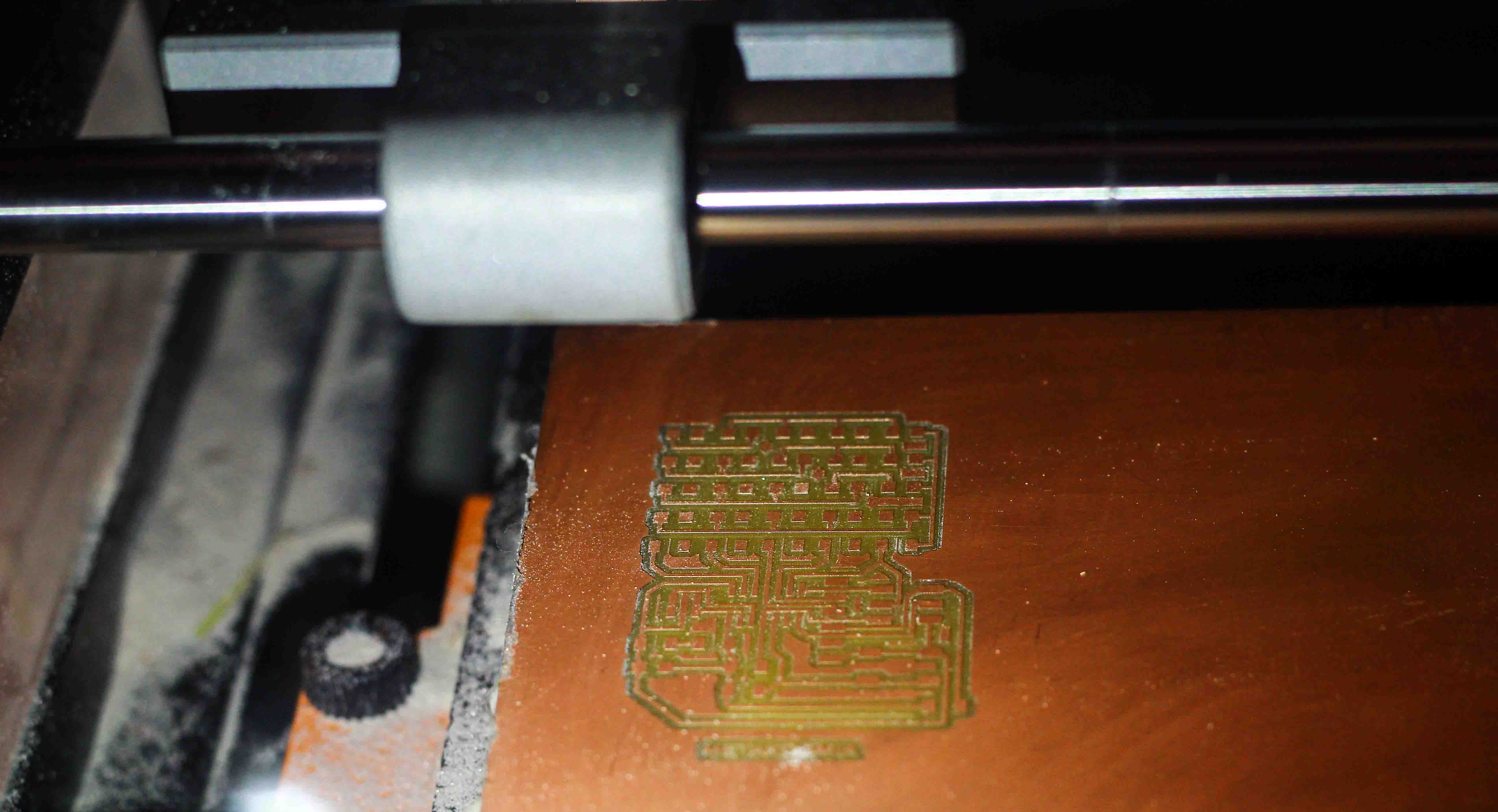
3. Milling the board without any short for the first time really feels good. I had some issue with the board and had to mill it again. These next versions weren't milling properly, felt like I ran out of luck.
Back to basics
A short amatuer guide to understanding electronics(more to be added)
I started with understand the basics of all the components. Next was to understand the pinout diagram of ATtiny 44.
The datasheet seemed alien to me and I had to shift to a different source to understand. But before that I had to understand
what a microcontroller(MCU) is and how it works. It is esentially as computer with a CPU, a memory, a system clock and few peripherals.
It is meant to perform specific tasks and find extensive application in embedded systems. Arduino is a great example of a MCU.
One can find MCU in cameras, microwave ovens and many other household electronics.
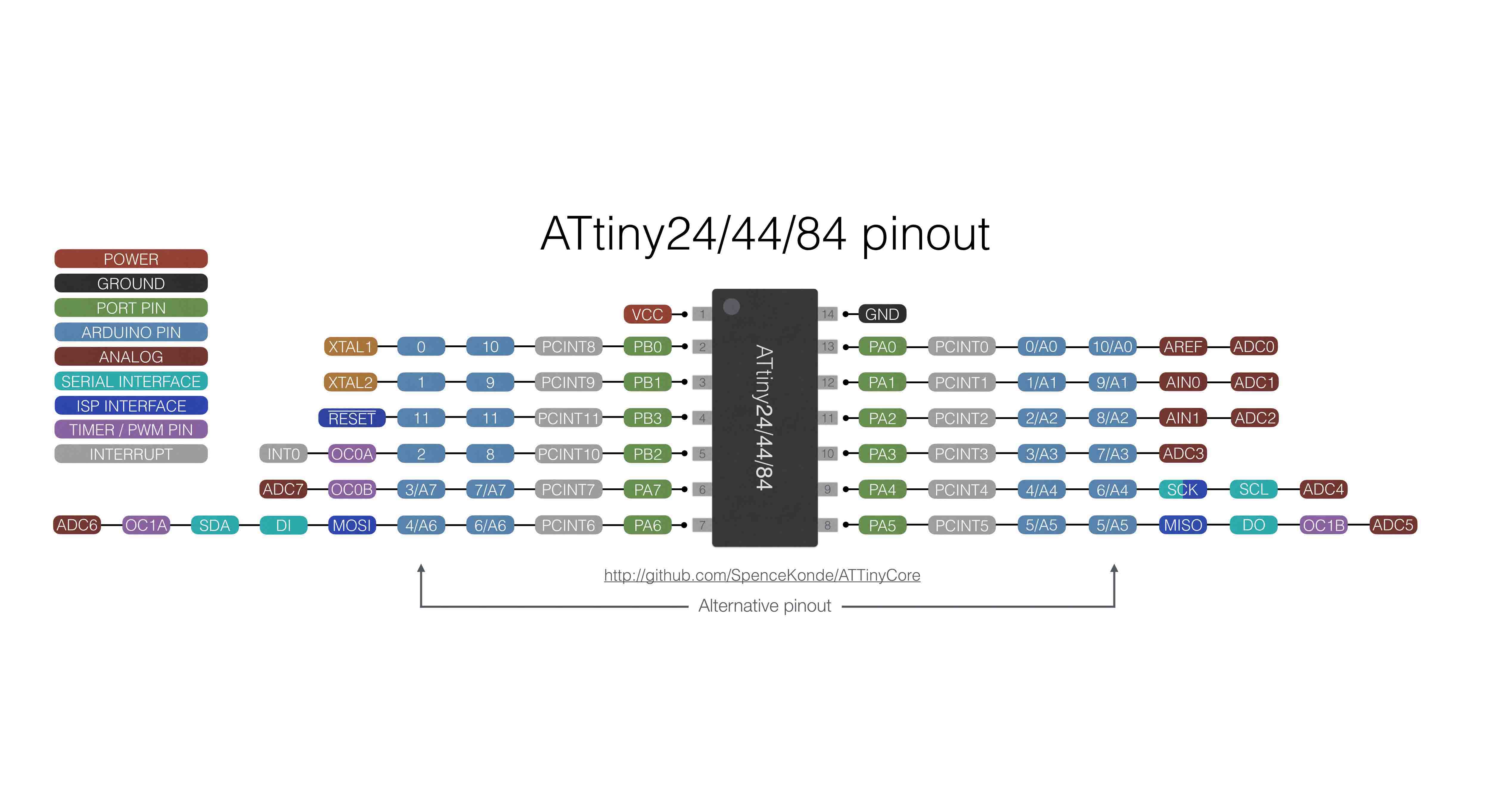
For someone like me who is not from an electronics background, understanding pinouts from datasheet initially was a nightmare and I religiously dedicated some time to understand it using various resources. I found a page on github that illustrates the pinout in a better way.Please find them here .
First Things First, there are pins and there are ports. A Pin is the physical metal part coming from the chip and
the number ascribed to it given its location on that chip. A Port refers to a Pin given its function within a register or the ports
are the I/O input/output channel connected internally to those pins. Furthermore, a
register could be understood here .
Next up, one would see an array of names labelled in a sequence expanding both
sides of the microcontroller pins. This is an alternative pinout diagram of the microcontroller(here ATtiny 44). To make it more
clear, lets take pin 13, its labelled as PA0, PCINT0, 0/A0, 10/A0, AREF and ADC0. This means that Pin 13 can be used as Port A 0(PA0),
Pin Change Interrupt 0 (PCINT0), Analog Reference (AREF) and Analog to Digital Converter (ADC0). One thing to mention here is that
Pin 13 is always Pin 13 but also Port 0 in the PA register.
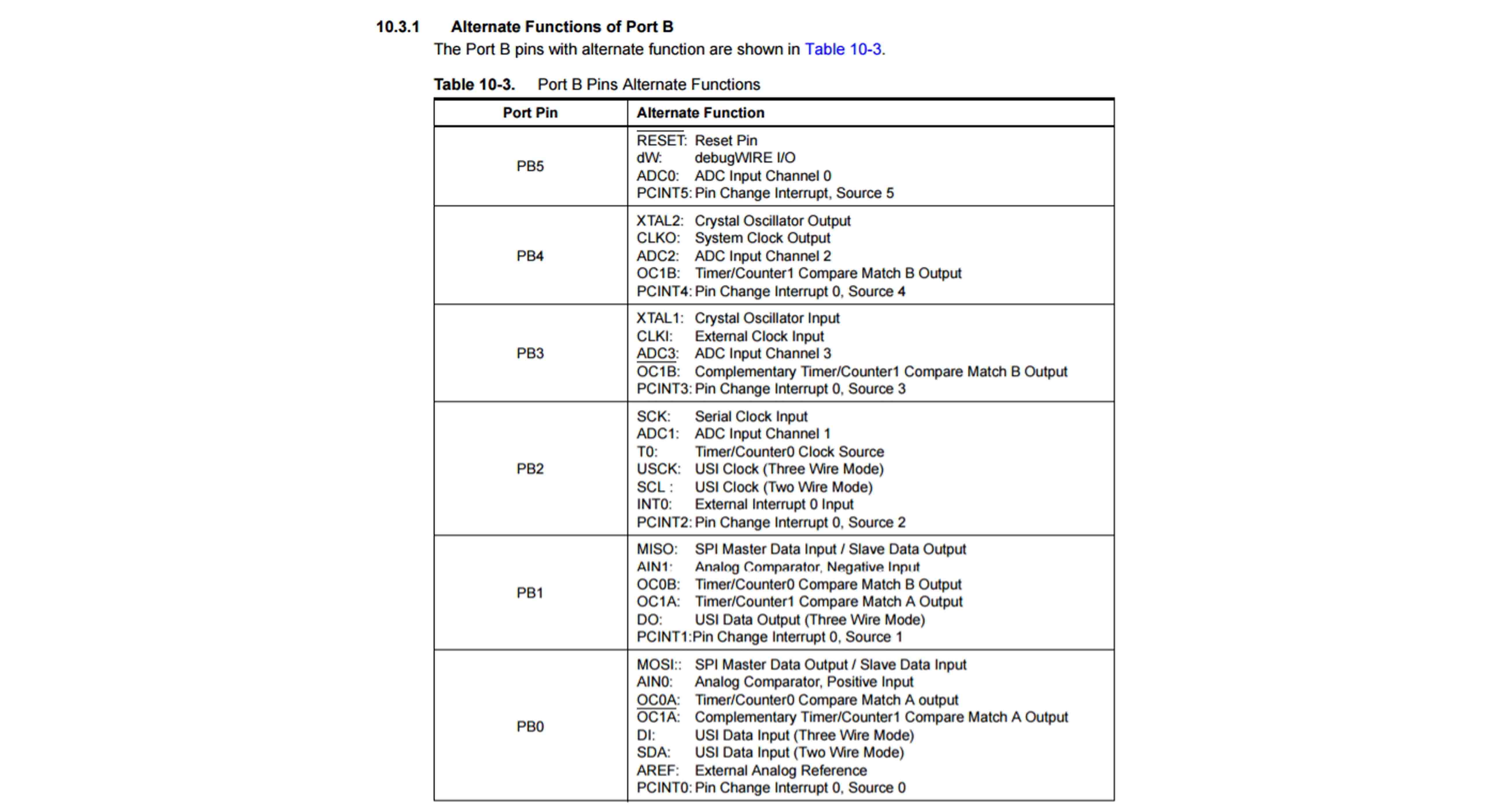
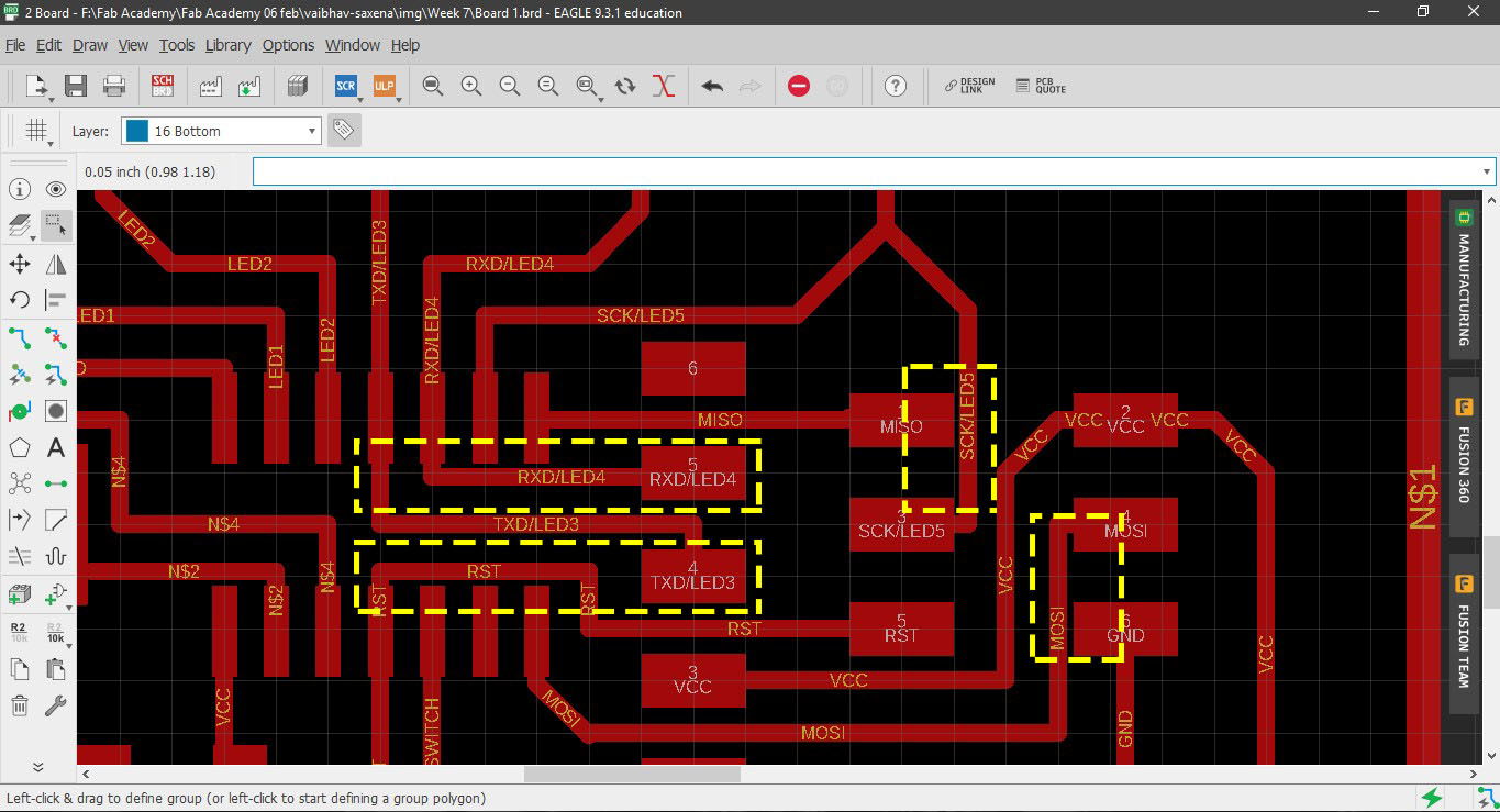
What is MISO, MOSI....?
As I was going through the Pinout diagram of the ATtiny 44, I came across MISO, MOSI, SCK alien terms and had to again look on the
internet, what these things mean. So a microcontroller uses Serial Peripheral Interface (SPI), a synchronous serial data protocol
used by microcontrollers for communicating with one or more peripheral devices quickly over short distances. It can also be used
for communication between two microcontrollers. With an SPI connection(Using a 2x3 pin header and connector) there is always one
master device (usually a microcontroller) which controls the peripheral devices.
MISO (Master In Slave Out) - The Slave line for sending data to the master,
MOSI (Master Out Slave In) - The Master line for sending data to the peripherals,
SCK (Serial Clock) - The clock pulses which synchronize data transmission generated by the master.
Three other lines that are present are VCC, GND and RESET or RST.
The SPI connection is also used to programme a programmer from a microcontroller.
One can also find MISO, MOSI, SCK, VCC, GND and RESET/RST on ATtiny 44 pinout diagram at pins 8, 7, 9, 1, 14 and 4. This link provides details in simple language here
Redesigning the "echo hello world" board with some spice
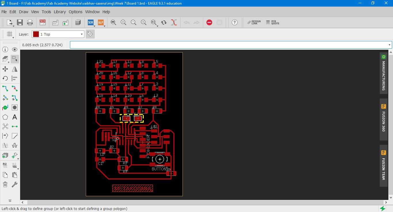
I chose Eagle over other softwares to design my PCB board because I had earlier(Week 5) tried using some basic features of the software
and found its UI to be very friendly.
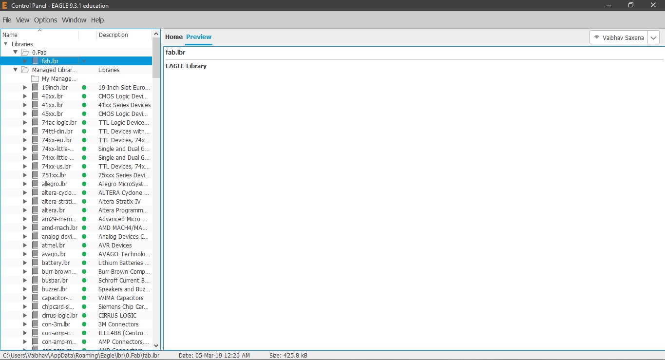
Next up, Fab network has created a library for EAGLE consisting of components commonly used in PCB design during the Fab Academy course.
1. Download the Fab library for Eagle here .
2. Place the downloaded file fab.lbr in C:\Users\Vaibhav\AppData\Roaming\Eagle\lbr. I created a folder named Fab in lbr folder and placed the fab.lbr file there.
3. Once you start EAGLE you will automatically see the fab.lbr in the control panel on the left side along with other predefined libraries.
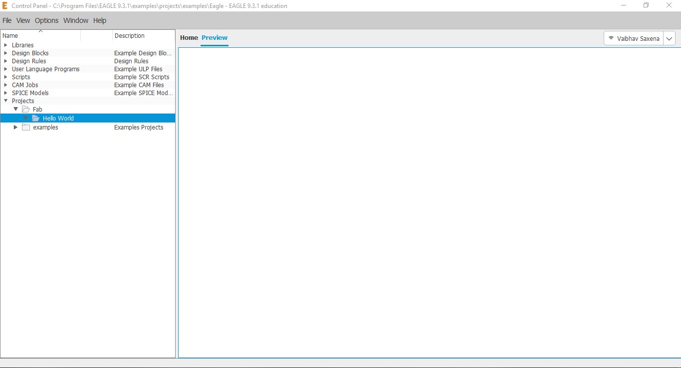
4. To get going initially, I downloaded the a sample schematic file from the Fab Academy tutorials.
5. Next up, I went into the Project directory of Eagle and created a new folder named Fab and inside that another folder named Hello World, to
keep the structure clean and keep my files for this assignment.
6. By right clicking on the folder "hello world", I create a new project and a new Schematic.
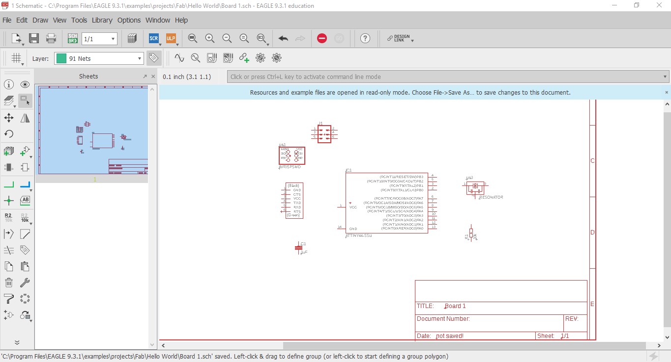
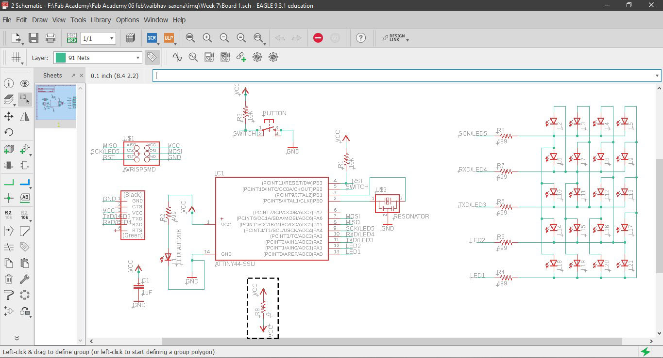
7. A schematic window opens up where we can draw the circuits without worrying about the component placement.
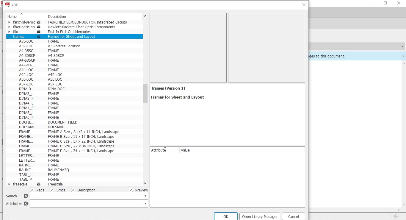
8. I started by adding a frame so that my circuit looks neat. This is done by either typing add or in the left tab, look for AddPart.
This will open a new window with the library and you can go to frames and choose the one you like depending on the size of your circuit.
9. One important tip while searching for components in the library. Use suffix *(wildcard on multiple characters) and ?(wildcard on
single character)
10. rcl library is highly used library in Eagle.
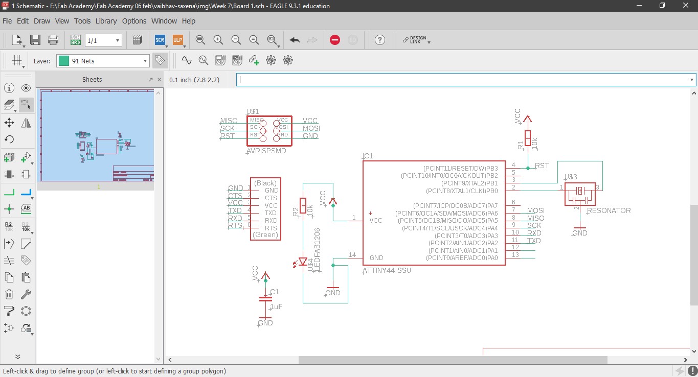
The basic components of the echo hello world board are:
ATTiny 44 as MCU x1
6 Pin AVR ISP Header x1
FTDI Header x1
20 MHz Resonator x1
1 uF Capacitor x1
10K Ohm Resistor x1
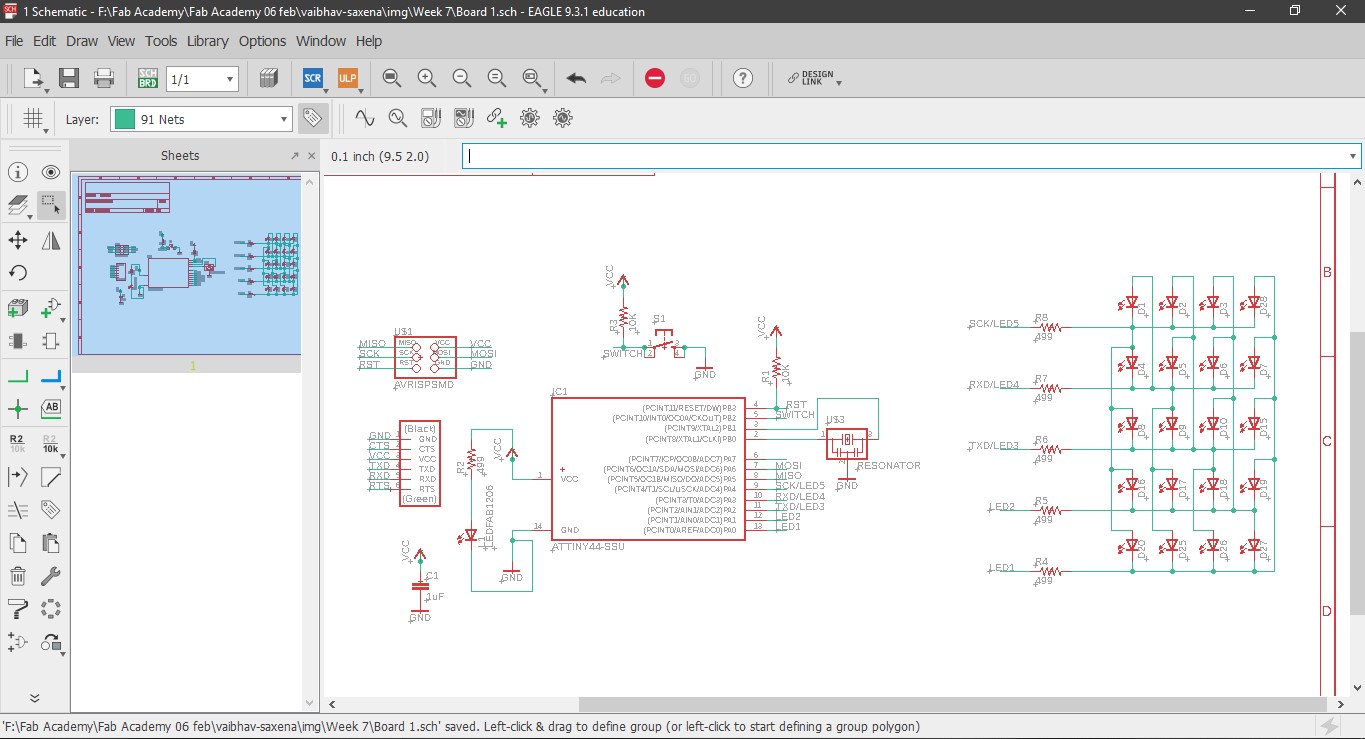
and I further added the following:
0K Ohm Resistor x1
Switch x1
Red LED for power x1
Green LED for Charlieplexing x20
499 Ohm resistor x5
The reset button resets the whole IC, it is by default in active high state. You can attach a switch button to reset it manually to active low state.
11. To make connections between the components, I extended a line from the individual components using NET tool and then typed the same unique name between
various components to join them. If one wants one can also label them.
12. Since I had a bad experience about how to know whether the PCB board is receiving power or not, hence I added one Red LED as soon the as the board receives power.
13. Now I wanted to play around a bit with input output and had few pins left on the ATtiny 44, hence I chose charlieplexing, a way to light up multiple LEDs in a cutomized pattern using fewer pins. I took reference of Nicolo Gnecchi's work, he has documented Charlieplexing beautifully. It can be found here .
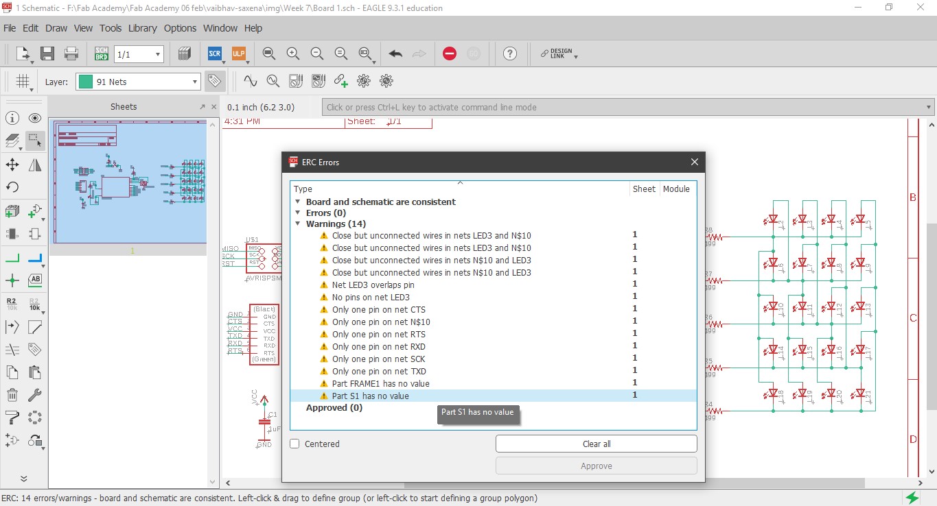
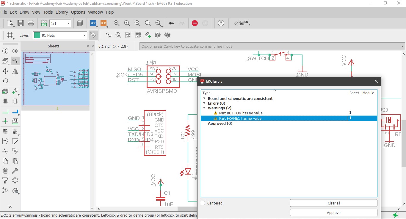
14. Before moving forward, an important step is to check whether all pins are connected or not. One might get some errors if some pins are unused, these can be ignored.
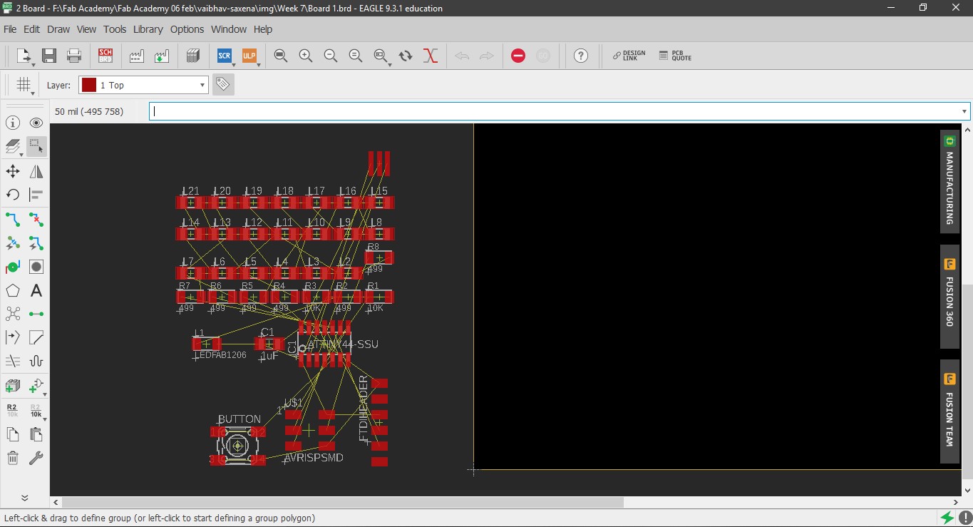
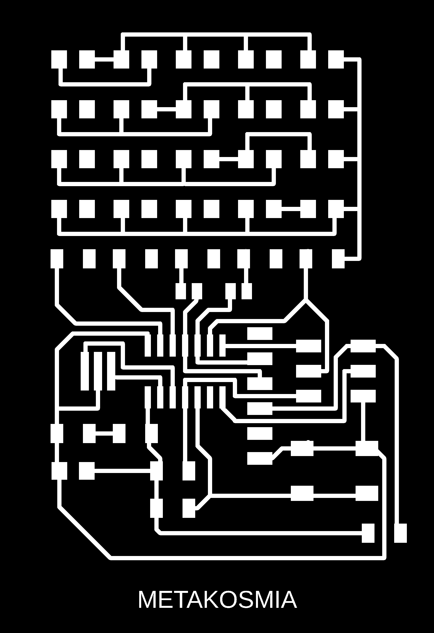
Routing and Designing the board
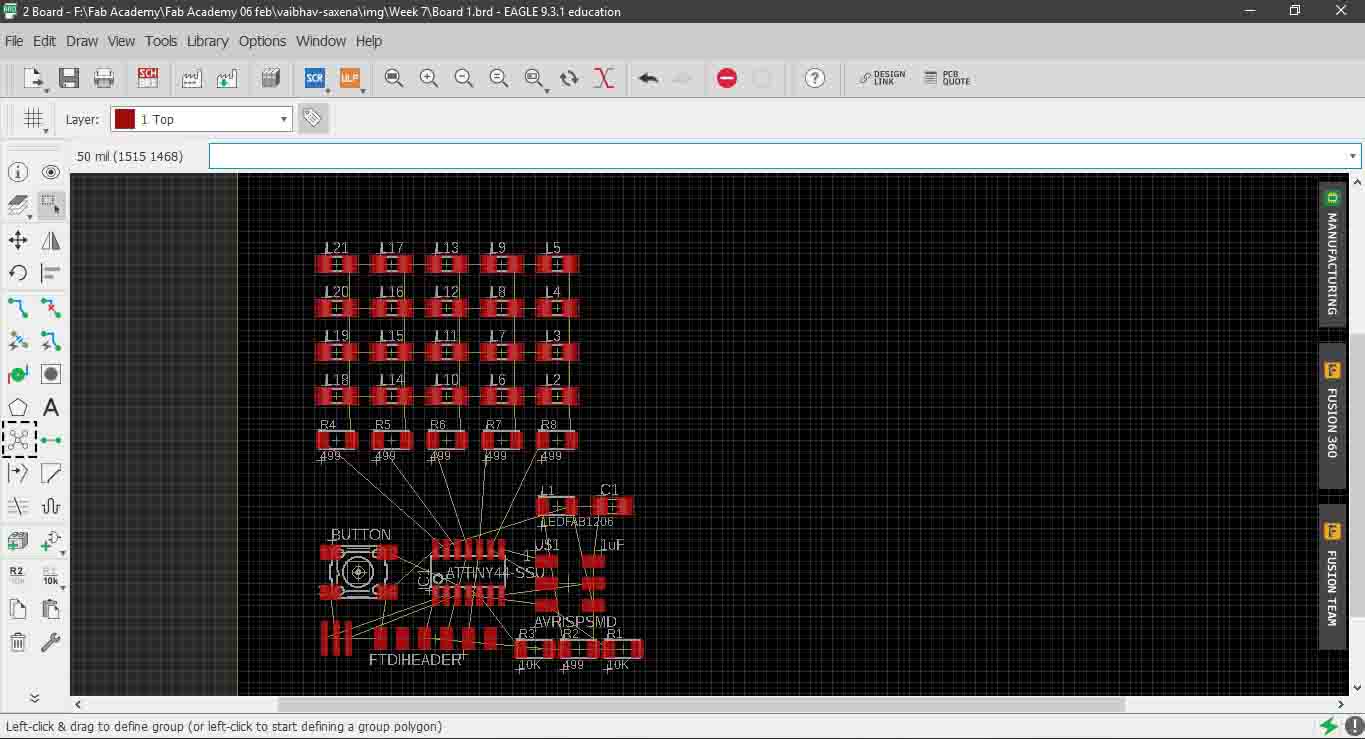
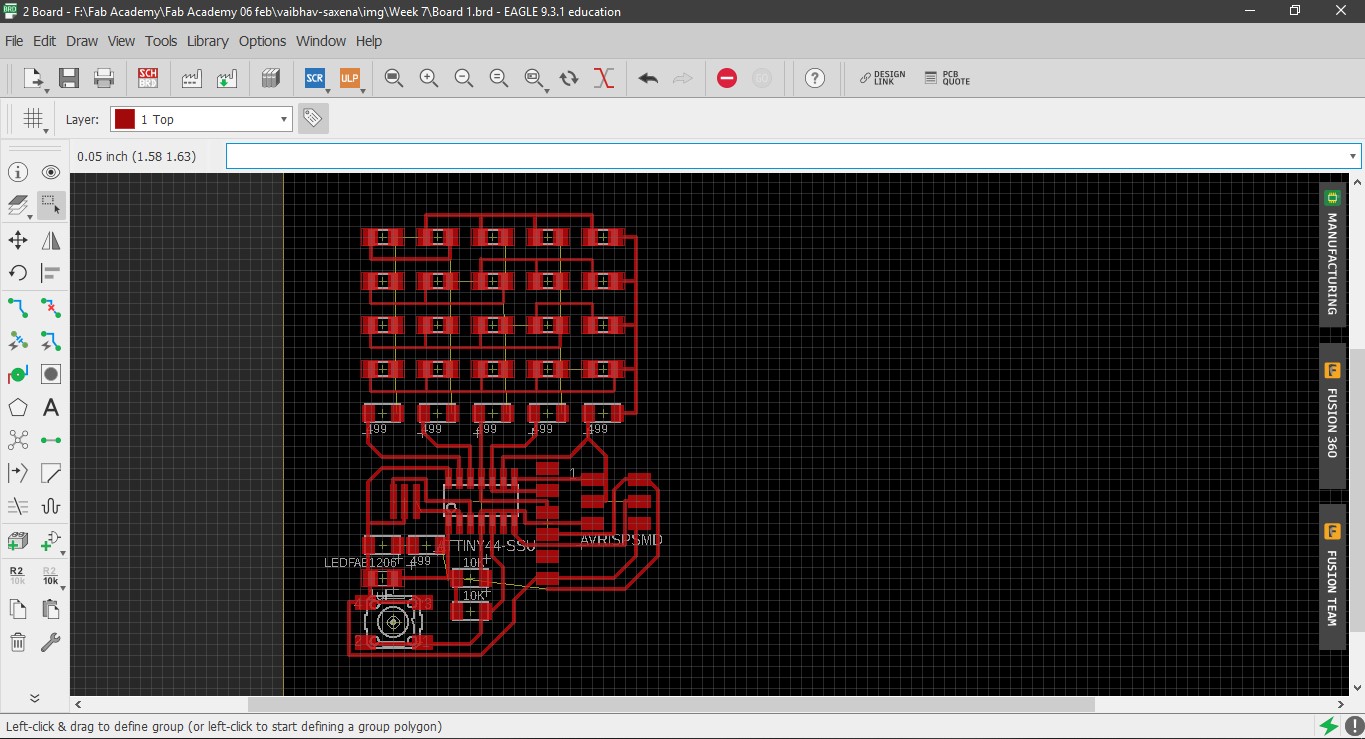
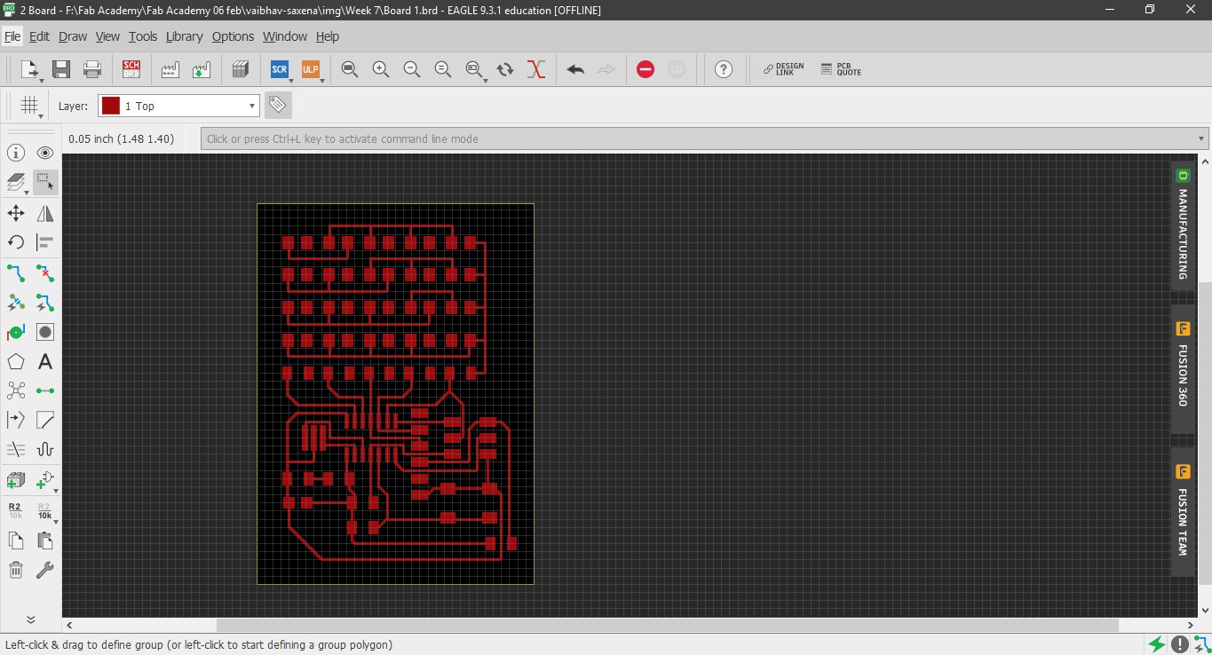

15. Next go to file and the click Switch to board, this opens up the board view in new window, here you can set the trace width and clearance, to name a few. The yellow
lines displayes the unrouted traces.
16. Select and move the components into the window. Also, the board view will show you suggestive connections called airwires.
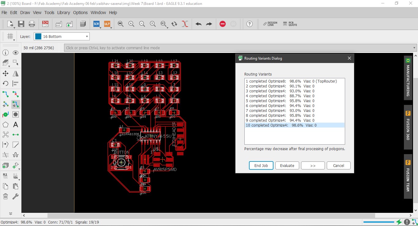
17 The way to solve routing is:
a)First solve the LED array grid.
b)Then fix the ATtiny 44.
c)Create GND such that it can connect components both inside as well as outside.
d)Do the same for VCC.
e) A golden tip would be use to autorouter when you have placed around 70-80% of your components. It will give you clues how to re-arrange the components.
If at any stage you want to remove a certain route got to Edit>Ripup or simply type ripup in the command line
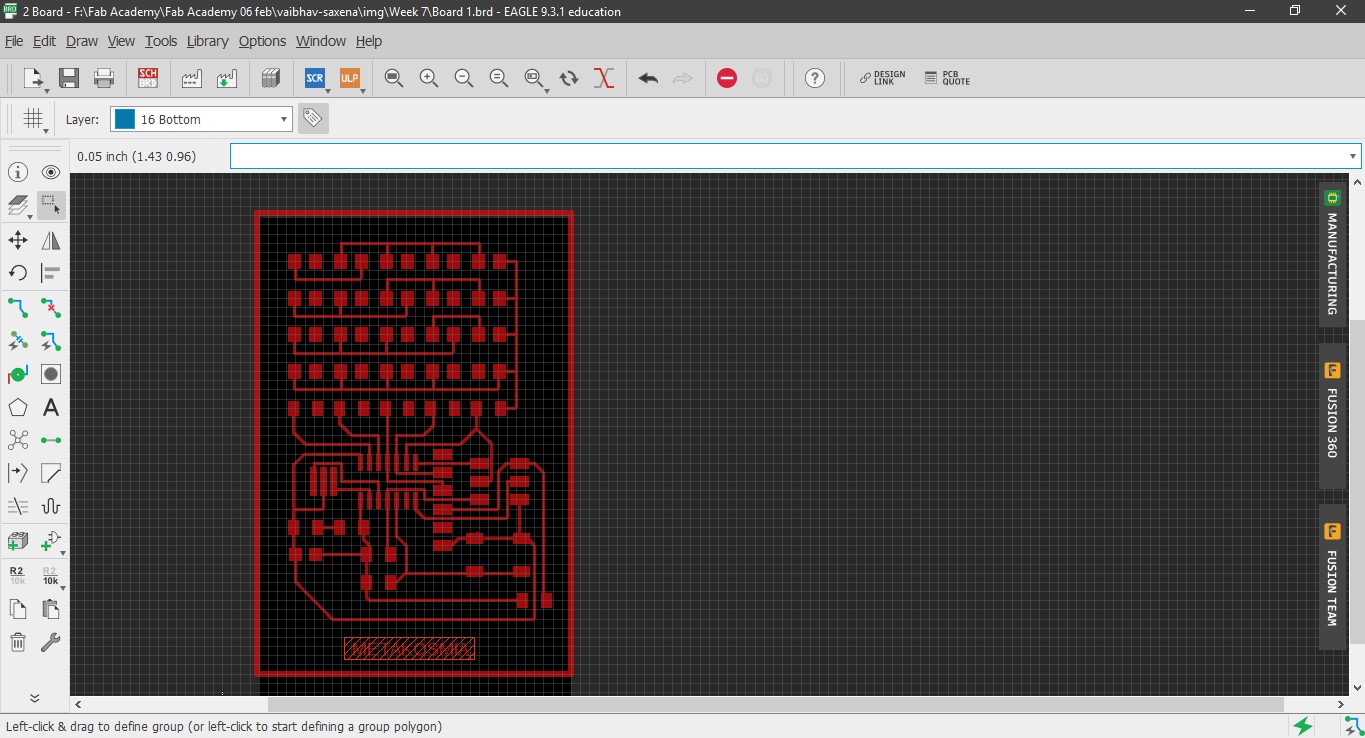
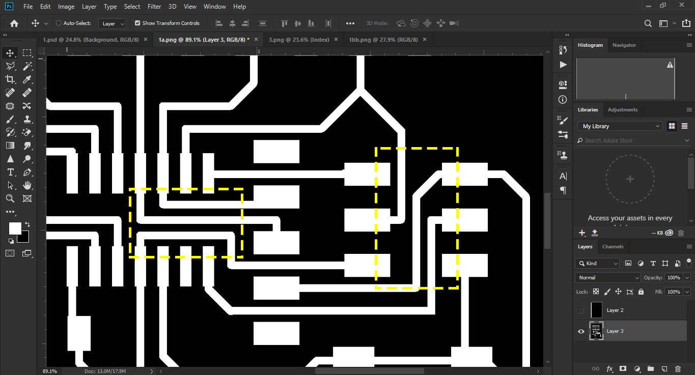
18. I made some major mistakes during routing the connections between LEDs of the the array. I forgot 4 series connections between the LEDs and due to shortage of time, had to make an alternative during soldering by overflowing extra solder between pads.
19. Finally a rule of thumb, the thickness of the traces should be 0.016 inch, this is neither too much nor too less. Also, keep the distance between two traces 0.016
inch. I used 1/64 inch on SRM-20 to mill my board and it came out pretty good.
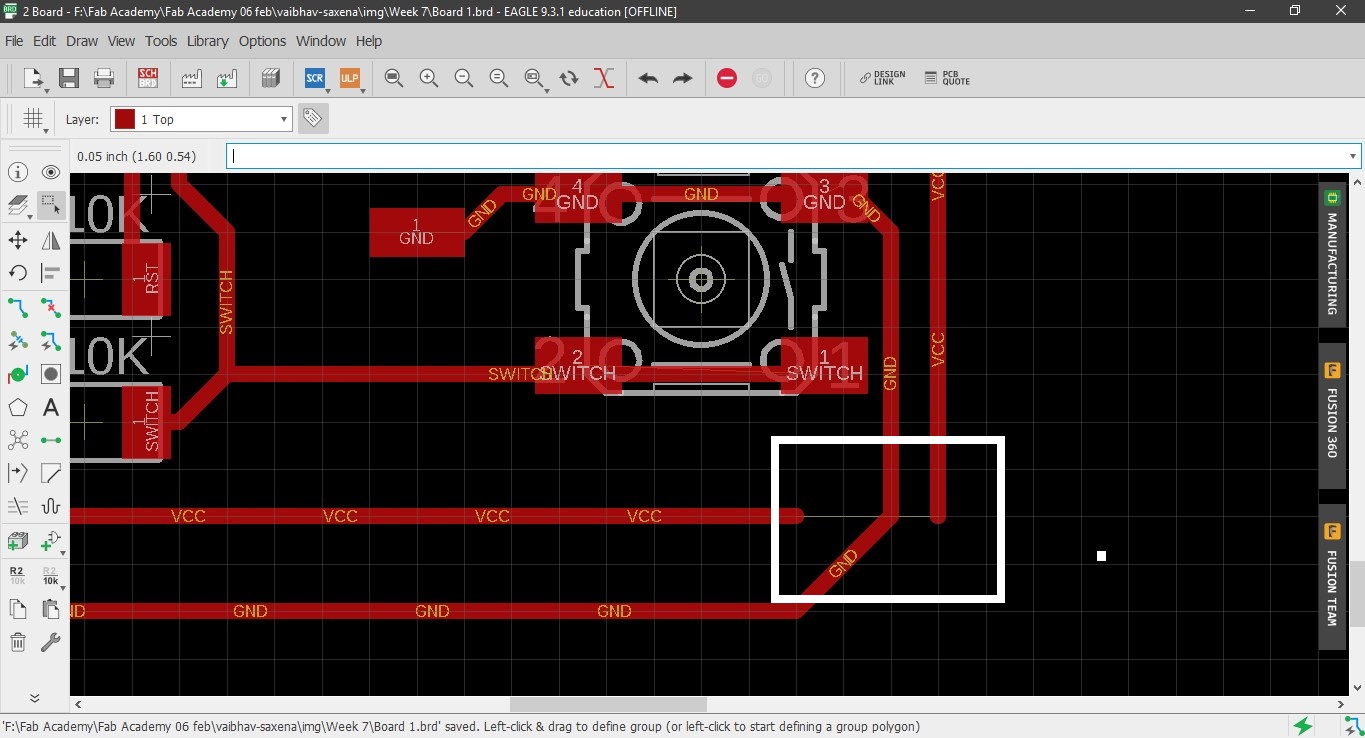
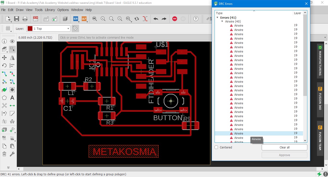
20. After finishing the routing, an important step is to check for Design Rules, by clicking DRC or just typing DRC in command line. This will show you possible errors. Not all errors are legible and many can be ignored depending on your PCB design. Another important thing to note here is that you can create your own design rules like minimum distance between traces and minimum thickness and so on.
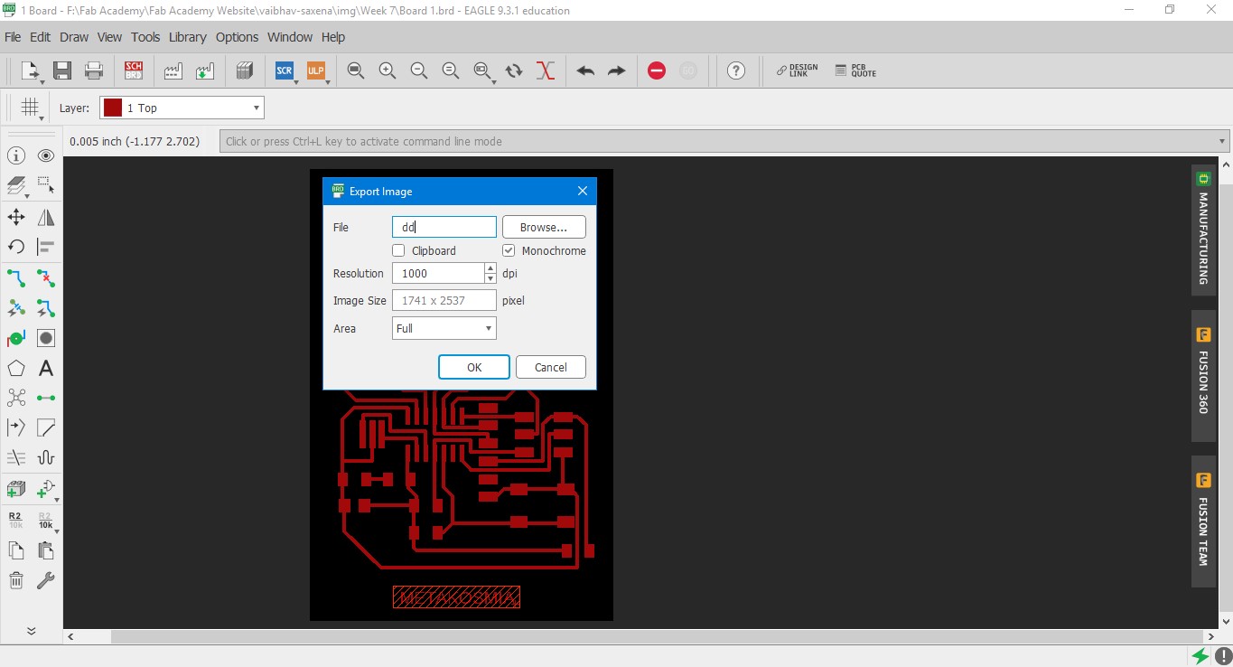
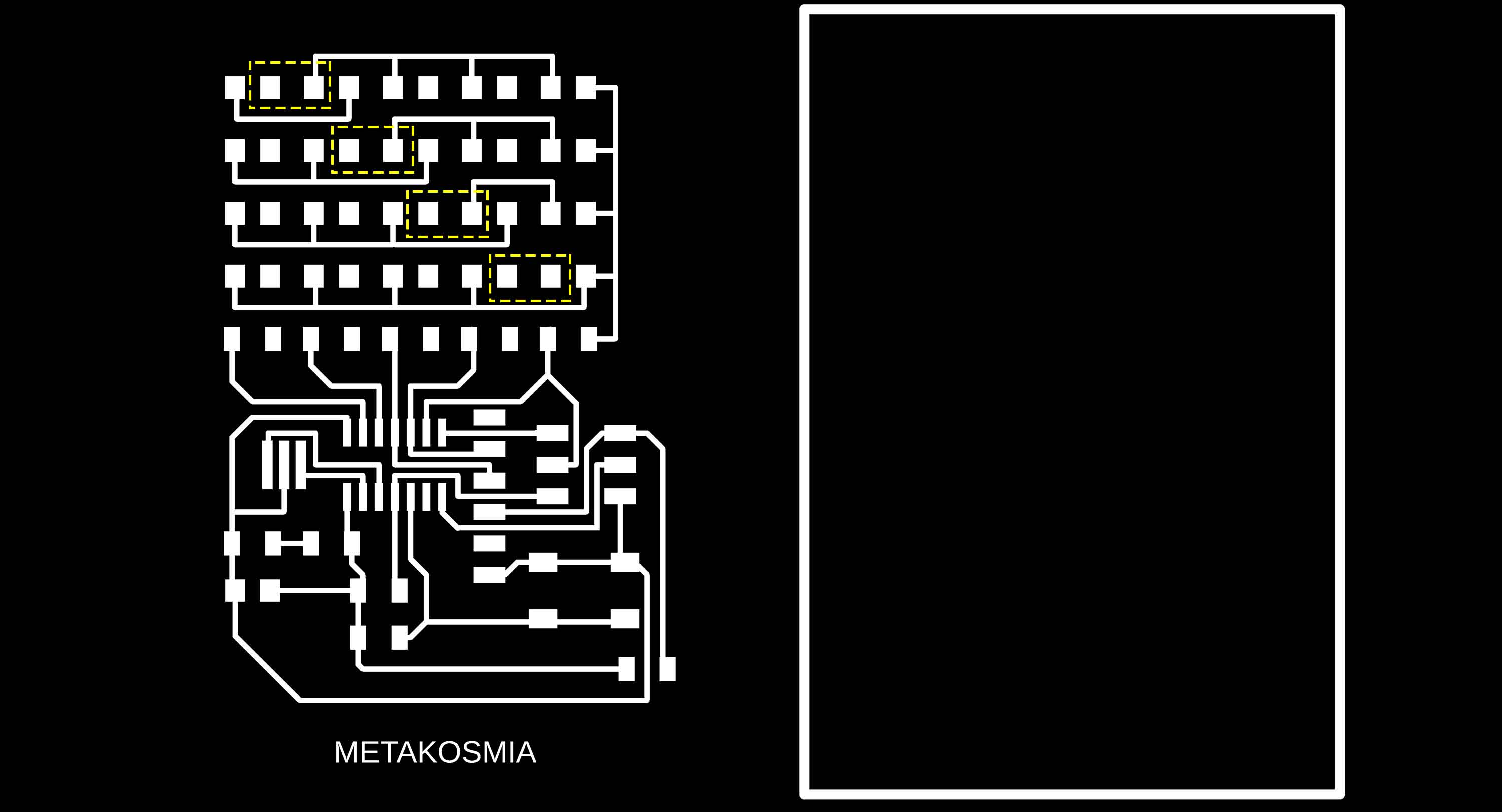
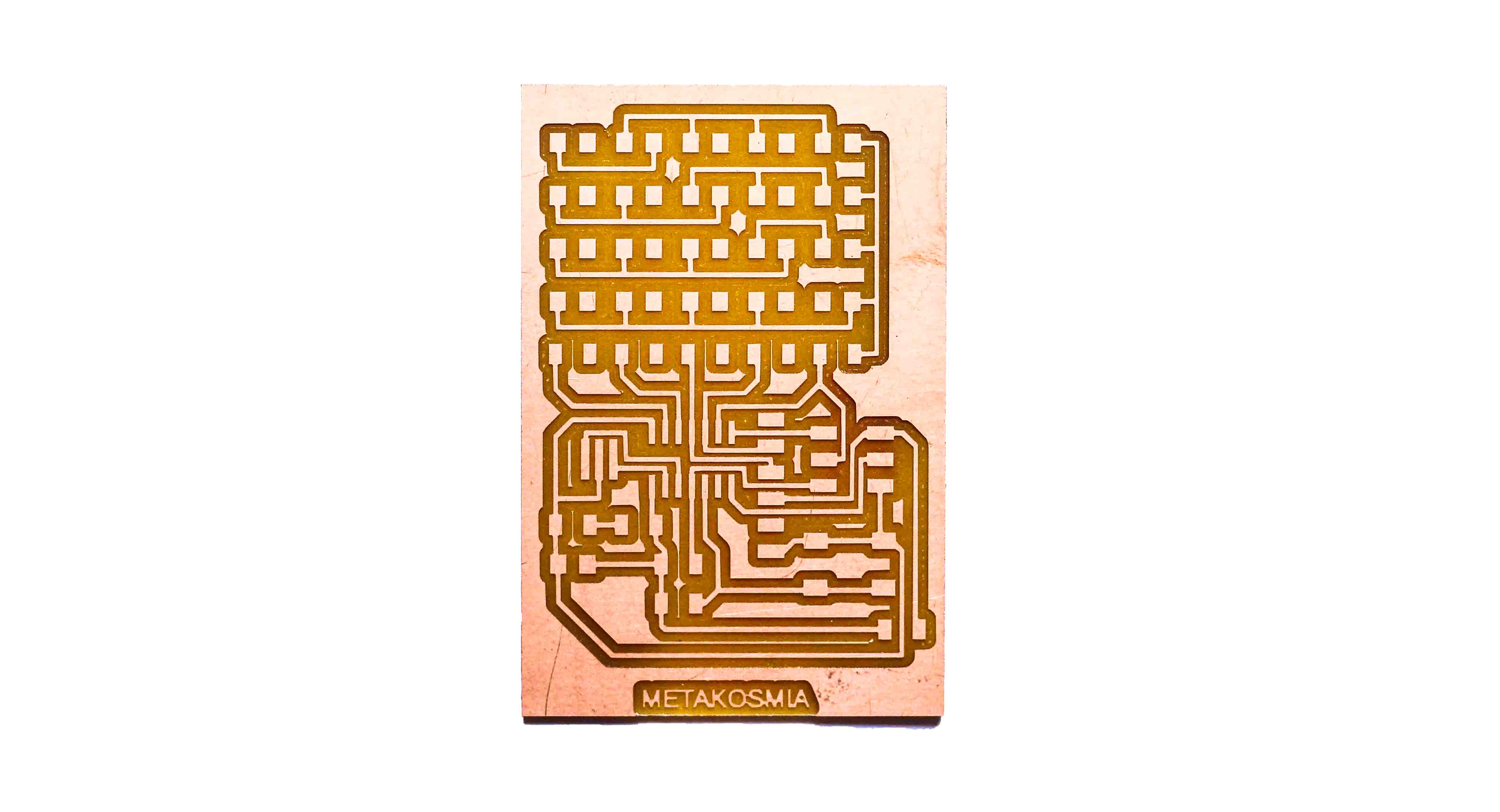
21. After removing the errors, we will hide all the layers except the top layer and export this file as .png for interior traces on milling machine. Go to File>Export>Image. Set the resolution to 1000 dpi and click on monochrome. Next, hide every layer and only keep dimension layer on and again export it .png. This is your profile trace to be cut on milling machine.
PCB milling and programming
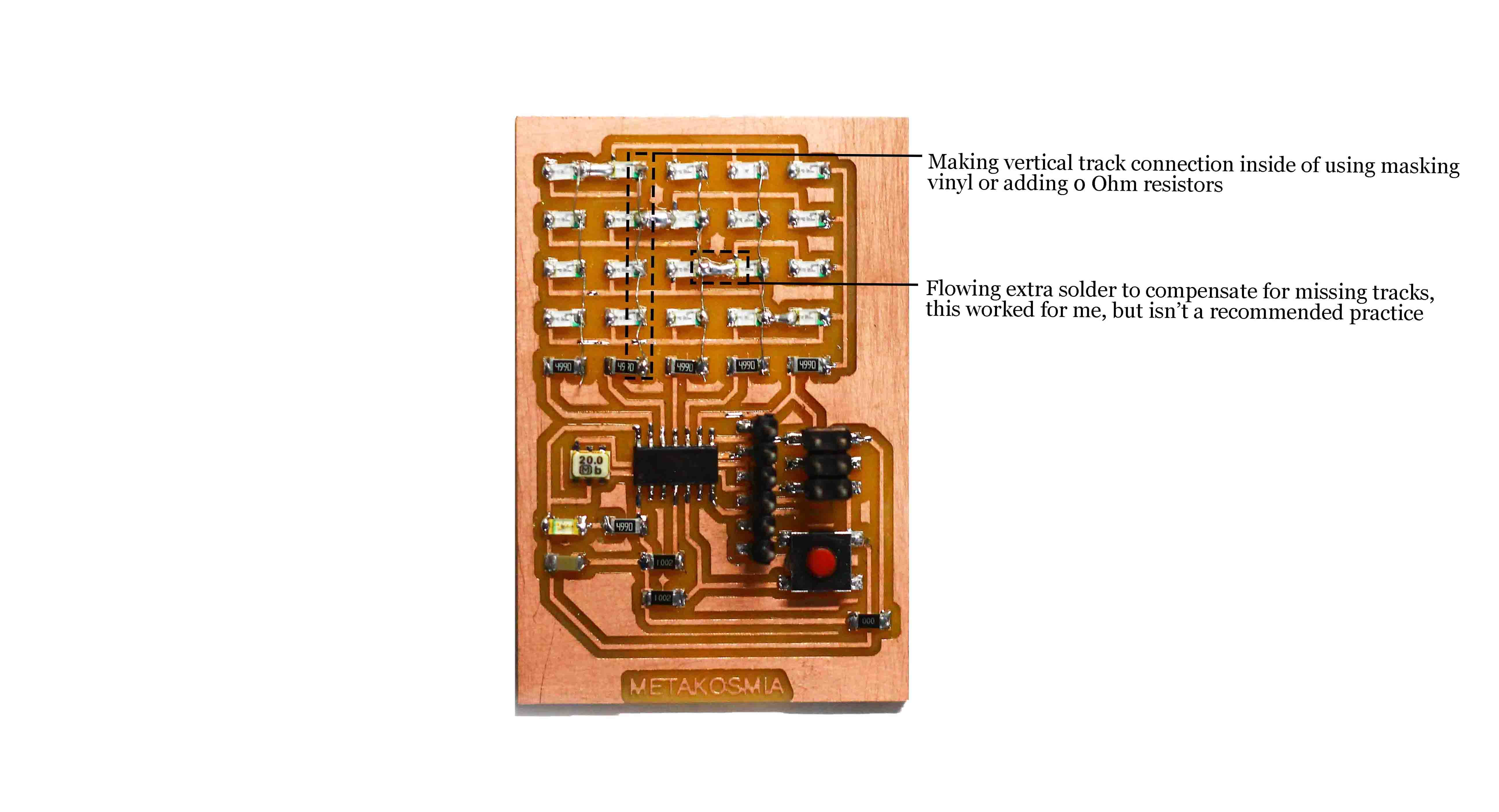
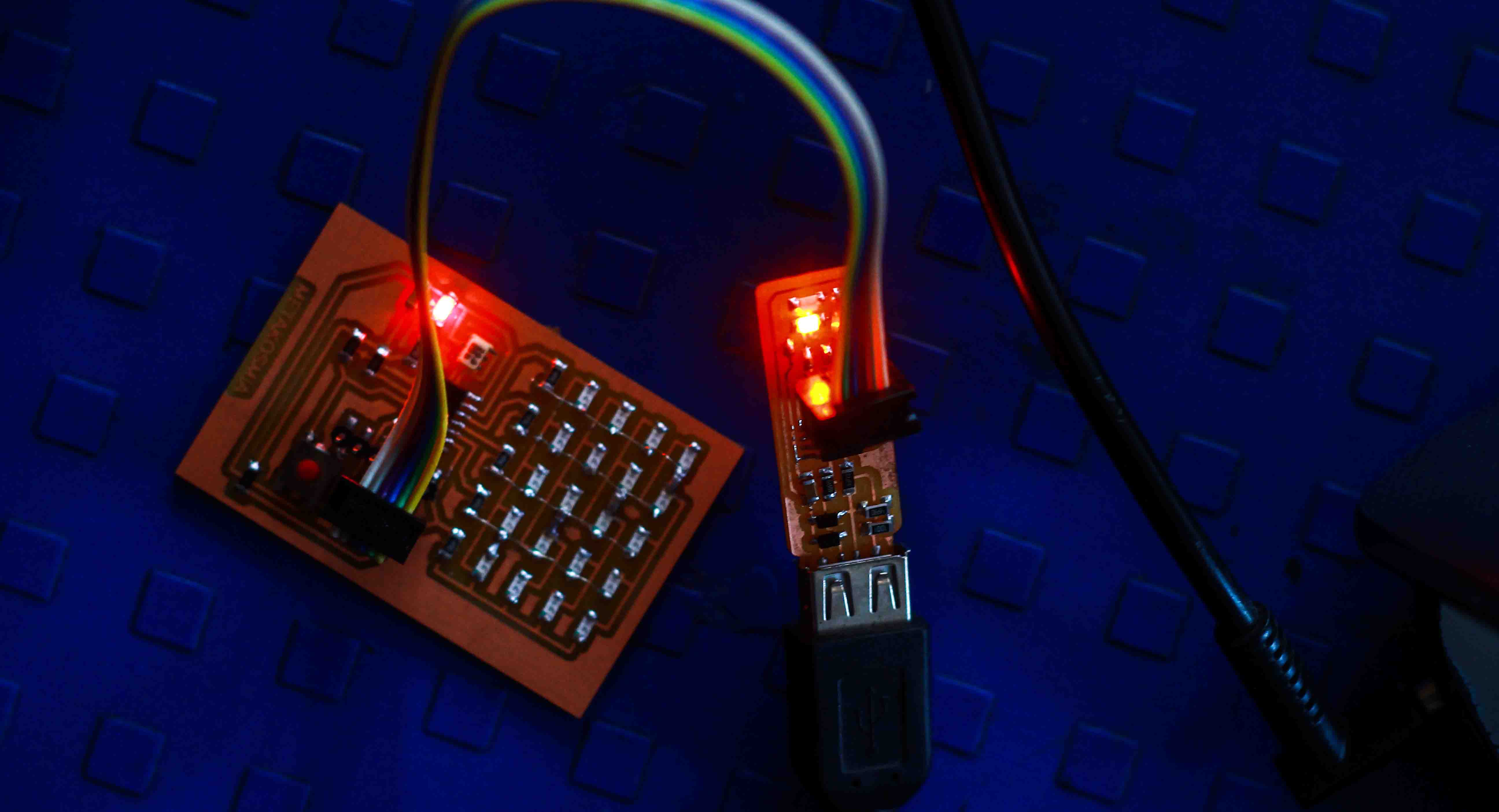
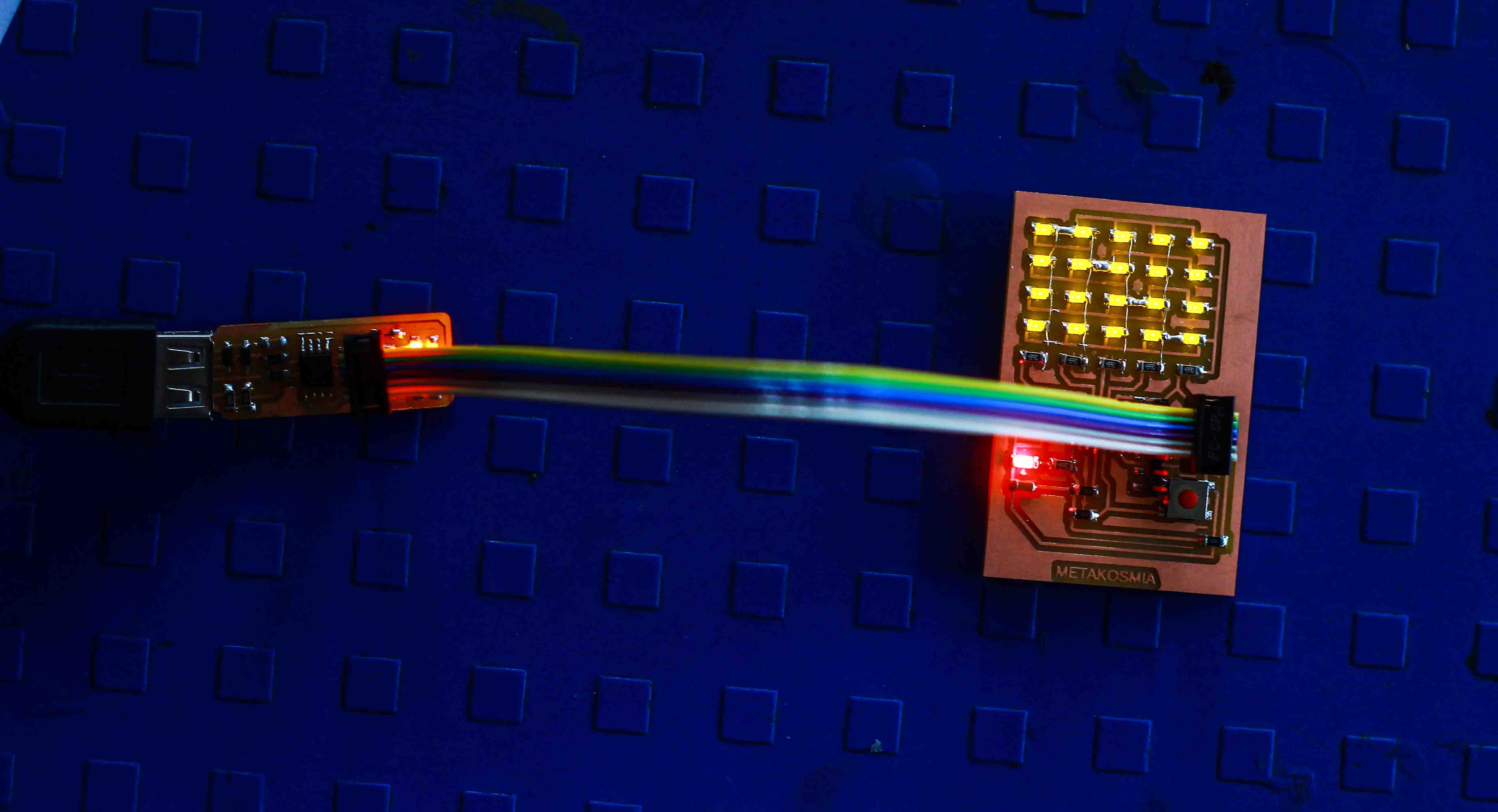
One of the important things with Charlieplexing is the issue of vertical traces between LEDs. I check some work done by people and there are usually two way to do it. First is by using 0 Ohm resistors like this and secondly using a masking Vinyl and soldering over it, like this. I took a new middle way out, by using a jumper wire and soldering it. Somehow, this looks much cleaner to me and goes unnoticed. See the illustration 4 above.
1. I tried to design my PCB board in such a way that it could run both
echo hello world as well as hello array (from week 13), but I couldn't run hello echo program due to some reasons.
Hence, I downloaded the "C" and "make" file for both from the individual weeks.
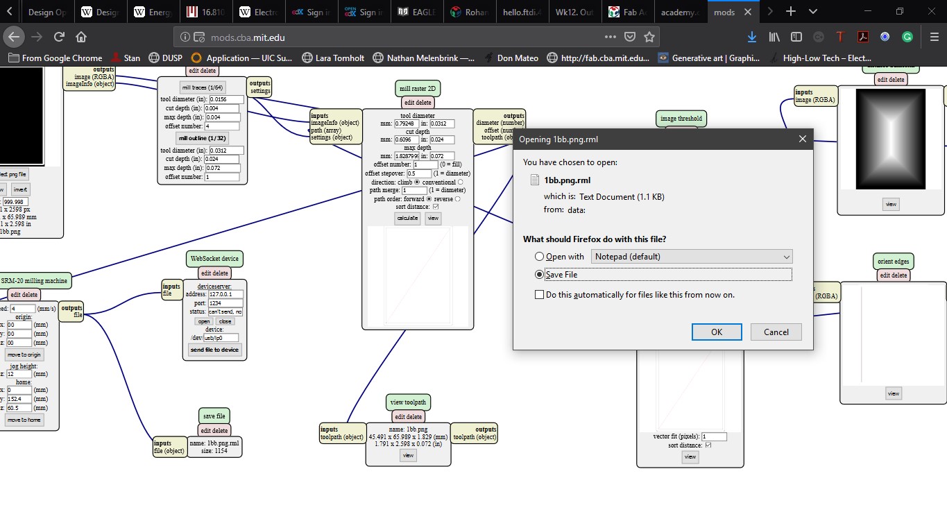
2. Since I am using windows, I will use Git Bash to execute the commands and programme my board. The link here helps in programming the board.
3. I opened GitBash from the same folder where I had saved C and make files.
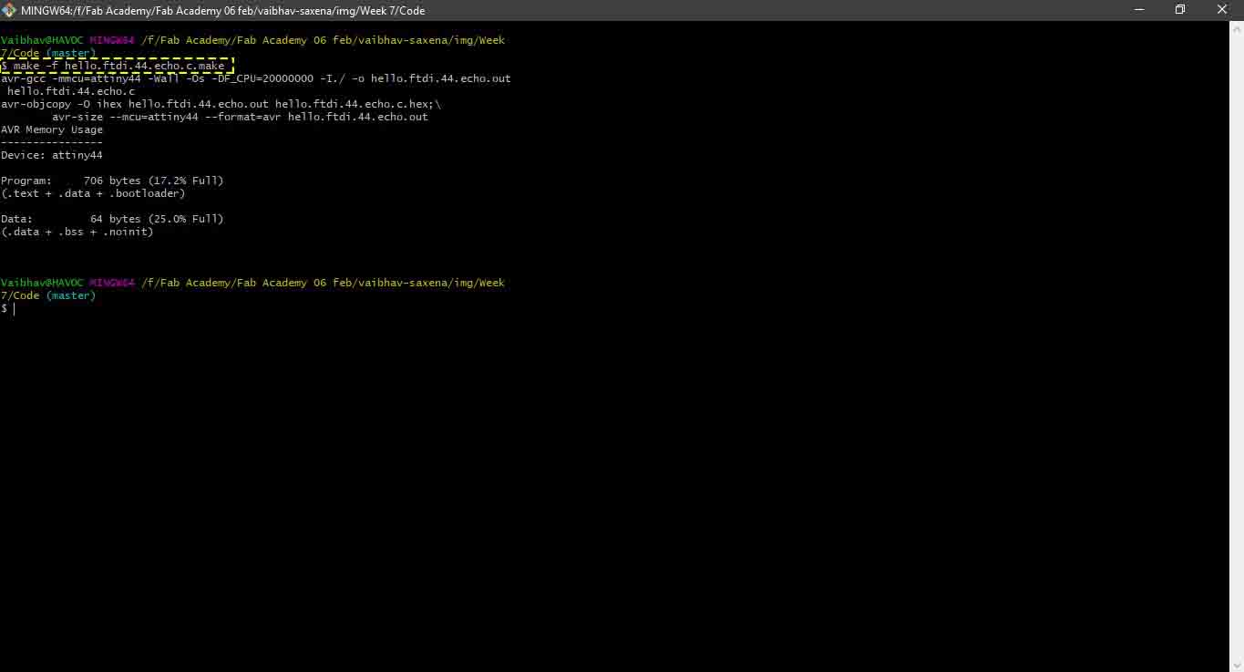
4. Execute, make -f hello.ftdi.44.echo.c.make, to compile the programme.
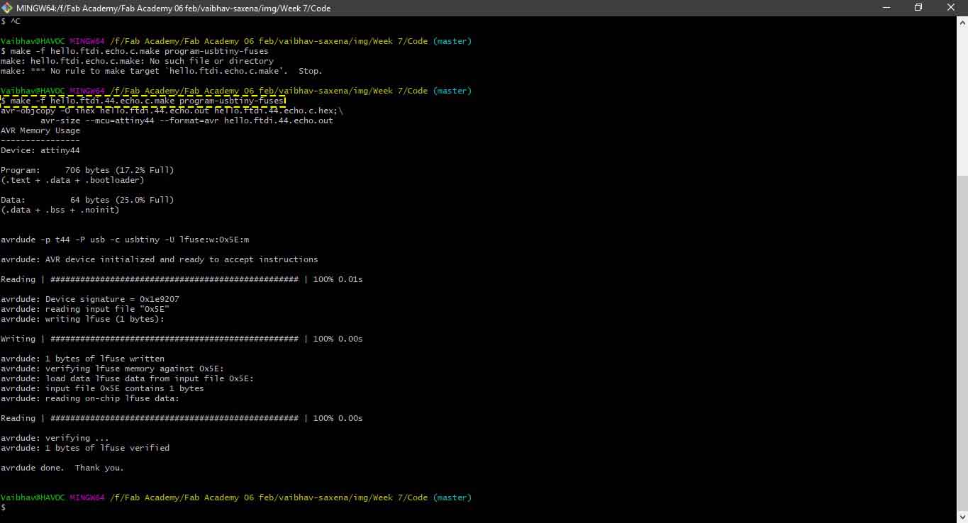
5. Execute, make -f hello.ftdi.44.echo.c.make program-usbtiny-fuses, to set the fuses. You should see avrdude done. Thank you. at the end.
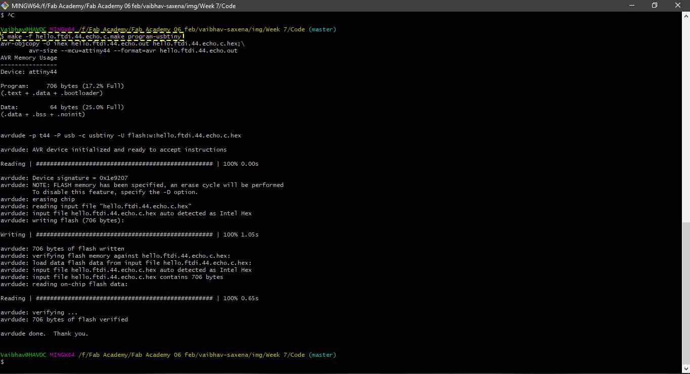
6. Execute, make -f hello.ftdi.44.echo.c.make program-usbtiny, this will flash the programme to the IC.
Furthermore, to check whether the board is responding to echo, I downloaded a slightly older version of python, python 2.7.
Now execute the command $python term.py /dev/ttyUSB0 115200. I did see a python window pop up which should start responding to whatever you type. But in my board somehow this wasn't happening. A possible error could have been due to the fact that RX TX was also connected to Resistors. Hence, this needed debugging and possibly a new board with jumpers.
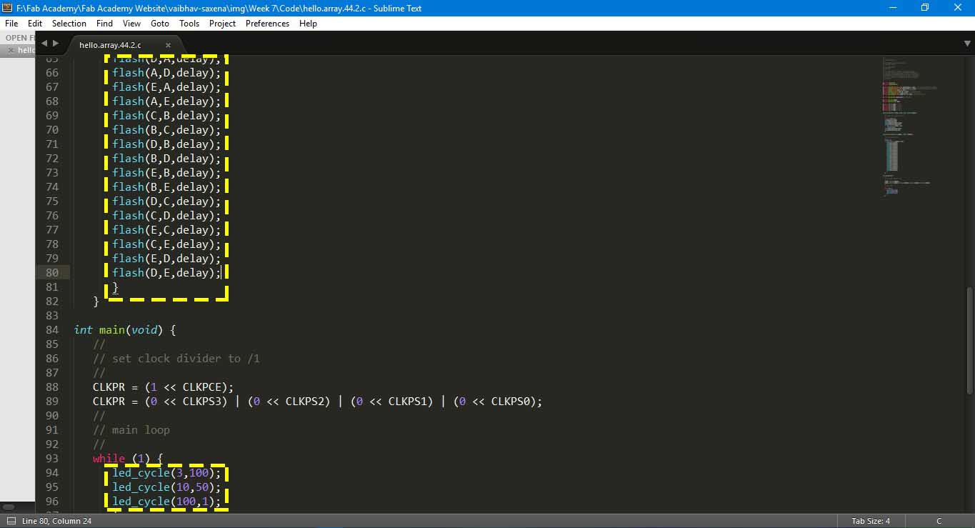
Now to run hello array follow the same steps above except that I renamed the file to hello.array.44.2.c.make
7. Execute, make -f hello.array.44.2.c.make, , to compile the programme.
8. Execute, make -f hello.array.44.2.c.make program-usbtiny-fuses
9. Execute, make -f hello.array.44.2.c.make program-usbtiny, this will flash the programme to the IC.
Once the above step is done for the hello array board, you can see a pattern flashing in the LEDs, this pattern can be further changed by editing the C file.(see the illustration above)
Download all the files for this week, here.
1. Schematic file
2. Board File
3. Final board_traces png file
4. Final board_outline png file
Group Assignment
The test equipment used to observe the operation of a microcontroller circuit board are:
1. Digital Voltmeter: A voltmeter is an instrument used for measuring electrical potential difference between two points in an electric circuit.
2. Oscillosope: An oscilloscope is a laboratory instrument commonly used to display and analyze the waveform of electronic signals.
3. Regulated Power Supply: